
アプリだけの便利な機能で
仕事探しがもっと快適に!
CONTROL
詳細を表示
半導体 - 熊本県菊陽町 の求人・仕事・採用
1,683件
詳細を表示
菊陽町 大字原水 / 原水駅 車8分
年収370万円 / 賞与・ボーナスあり
正社員

- 研修あり
- 交通費支給
- 未経験OK
- 平日休み
- シフト制
- 特別休暇
- 夜勤
- 交替勤務制
- U・IターンOK
- 職場内禁煙
- 雇用保険完備
- 厚生年金加入
- 住宅手当あり
- 産休・育休実績あり
- 介護休暇あり
- 寮完備
- 資格取得支援制度
- 学歴不問
半導体オペレーター
非公開
菊陽町
月給26万円〜47万円 / 昇給あり
正社員
週休2日制 / 1日4時間以内OK

- 若手活躍中
- 研修あり
- 社会保険完備
- 未経験OK
- 交通費支給
- シフト制
- 特別休暇
- 長期
- 残業手当あり
- キャリアアップ制度
- 雇用保険完備
- 厚生年金加入
- 資格取得支援制度
- 制服貸与
- 冷暖房完備
- 休憩室あり
- WEB面接OK
- スキルアップ
- 教育充実
半導体工場の運転管理業務
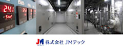
株式会社JMテック(ジャパンマテリアルグループ)
菊陽町 大字原水
年収440万円 / 賞与・昇給あり
正社員
週休2日制

- 資格取得支援制度
- 社会保険完備
- 長期休暇あり
- 年間休日120日以上
- 昇格あり
- 交通費支給
- 車通勤OK
- キャリアアップ制度
- 雇用保険完備
- 厚生年金加入
- 家族手当あり
- 住宅手当あり
- 未経験OK
- 福利厚生充実
- 有資格者歓迎
- スキルアップ
- 資格不問
菊陽町
月給21万円〜30万円 / 賞与・昇給あり
正社員

- 研修あり
- 社会保険完備
- 資格取得支援制度
- 交通費支給
- シフト制
- 長期休暇あり
- 夜勤
- 交替勤務制
- 転勤なし
- 退職金制度あり
- 残業手当あり
- 車通勤OK
- 職場内禁煙
- 雇用保険完備
- 厚生年金加入
- 寮完備
- 食事補助あり
- スキルアップ
製造スタッフ/半導体製造装置のボタン操作や見守り・検査
株式会社フジワーク
菊陽町 大字原水 / 原水駅 徒歩40分
時給1,400円 / 賞与・昇給あり
契約社員
完全週休2日制

- 若手活躍中
- ミドル活躍中
- 研修あり
- 未経験OK
- 交通費支給
- 社会保険完備
- 寮完備
- 高収入
- 週払いOK
- 平日休み
- シフト制
- 長期休暇あり
- 年間休日120日以上
- 特別休暇
- 第二新卒歓迎
- 交替勤務制
- U・IターンOK
- 転勤なし
- BtoB
- 自社サービス
- 理系歓迎
- 退職金制度あり
- 残業手当あり
- 正社員登用あり
- バイク通勤OK
- 車通勤OK
- 自転車通勤OK
- 職場内禁煙
- ノルマなし
- 駐車場あり
- 家族手当あり
- 住宅手当あり
- 介護休暇あり
- 資格取得支援制度
- 冷暖房完備
- 福利厚生充実
- 急募
- 学歴不問
- スキルアップ
- 資格不問
- スキル不問
- マネージャー採用
半導体製造装置の保守・保全業務
熊本県菊池郡菊陽町 大手半導体デバイスメーカー
菊陽町 大字原水
月給21万円〜35万円 / 賞与・昇給あり
正社員
週休3日制

- 研修あり
- 社会保険完備
- 資格取得支援制度
- 交通費支給
- シフト制
- 年間休日120日以上
- 特別休暇
- 長期
- 夜勤
- 退職金制度あり
- 残業手当あり
- 正社員登用あり
- バイク通勤OK
- 車通勤OK
- 職場内禁煙
- 雇用保険完備
- 厚生年金加入
- 家族手当あり
- 住宅手当あり
- 祝い金あり
- 介護休暇あり
- 未経験OK
- 寮完備
- 制服貸与
- 冷暖房完備
- 初心者歓迎
- WEB面接OK
- 友達と応募OK
- 学歴不問
- 資格不問
- 教育充実
どの働き方をご希望ですか?
半導体(メンテナンス)/半導体製造装置のメンテナンス・修理
株式会社フジワーク
菊陽町 大字原水 / 原水駅 徒歩40分
月給22万円 / 賞与・昇給あり
正社員
完全週休2日制

- 若手活躍中
- ミドル活躍中
- 研修あり
- 交通費支給
- 社会保険完備
- 平日休み
- シフト制
- 週休2日制
- 長期休暇あり
- 年間休日120日以上
- 特別休暇
- 第二新卒歓迎
- 夜勤
- 交替勤務制
- U・IターンOK
- 転勤なし
- BtoB
- 自社サービス
- 理系歓迎
- 退職金制度あり
- 残業手当あり
- バイク通勤OK
- 車通勤OK
- 自転車通勤OK
- 職場内禁煙
- 家族手当あり
- 住宅手当あり
- 産休・育休実績あり
- 介護休暇あり
- 未経験OK
- 寮完備
- 資格取得支援制度
- 制服貸与
- 急募
- 学歴不問
- スキルアップ
- 資格不問
- スキル不問
- 職歴不問
半導体分野のサービスエンジニア/未経験歓迎/月給34万円~
サイマー・ジャパン株式会社
菊陽町
年収465万円 / 賞与・昇給あり
正社員
土日休み / 完全週休2日制 / 残業月20時間以内
- 研修あり
- 社会保険完備
- 未経験OK
- スキルアップ
- 交通費支給
- 年間休日120日以上
- 特別休暇
- 第二新卒歓迎
- 夜勤
- U・IターンOK
- 直行直帰あり
- 転勤なし
- 退職金制度あり
- 残業手当あり
- 車通勤OK
- 雇用保険完備
- 厚生年金加入
- WEB面接OK
- AT限定OK
- 教育充実
半導体前工程のプロセス最適化
株式会社オープンアップネクストエンジニア
菊陽町
月給30万円〜55万円 / 賞与・昇給あり
正社員
完全週休2日制 / 残業月20時間以内

- 研修あり
- 社会保険完備
- 交通費支給
- 資格取得支援制度
- スキルアップ
- 年間休日120日以上
- 無期雇用派遣
- 特別休暇
- 退職金制度あり
- 残業手当あり
- 雇用保険完備
- 厚生年金加入
- 祝い金あり
- 介護休暇あり
- 未経験OK
- 赴任旅費支給
- WEB面接OK
- 経験者優遇
- 語学を活かせる
半導体工場のガス供給管理業務
株式会社JMテック(ジャパンマテリアルグループ)
菊陽町 大字原水
年収480万円 / 賞与・昇給あり
正社員
- シフト制
- 夜勤
- 交替勤務制
- 昇格あり
- 残業手当あり
- 交通費支給
- 車通勤OK
- キャリアアップ制度
- 雇用保険完備
- 厚生年金加入
- 社会保険完備
- 家族手当あり
- 住宅手当あり
- 未経験OK
- 資格取得支援制度
- 福利厚生充実
- 有資格者歓迎
- スキルアップ
- 資格不問
半導体工場施工管理
非公開
菊陽町
月給25万円〜45万円 / 賞与・昇給あり
正社員
週休2日制 / 1日4時間以内OK

- 研修あり
- 資格取得支援制度
- 社会保険完備
- 未経験OK
- シフト制
- 長期休暇あり
- 年間休日120日以上
- 特別休暇
- 長期
- 17時までに退社可
- 残業手当あり
- 交通費支給
- 雇用保険完備
- 厚生年金加入
- 寮完備
- ブランクOK
- 制服貸与
- 学歴不問
- スキルアップ
- 資格不問
- 教育充実
半導体製造装置のエンジニア/年休120日/U・Iターン歓迎
DAS Environmental Equipment Japan合同会社
菊陽町
年収300万円 / 賞与・昇給あり
正社員
完全週休2日制 / 残業月20時間以内
- 社会保険完備
- 交通費支給
- 長期休暇あり
- 年間休日120日以上
- 特別休暇
- 18時までに退社可
- U・IターンOK
- 転勤なし
- 海外出張あり
- 外資系企業
- 大手企業
- 残業手当あり
- 車通勤OK
- 職場内禁煙
- 雇用保険完備
- 厚生年金加入
- 介護休暇あり
- 未経験OK
- 英語を活かせる
- 中国語を活かせる
- 語学を活かせる
半導体製品製造装置オペレーター/「未経験歓迎」注目の半導体 まっさらでも大丈夫
株式会社フジワーク 熊本事業所
菊陽町 大字原水 / 原水駅 車8分
時給1,400円
契約社員
- 研修あり
- 未経験OK
- 交通費支給
- 社会保険完備
- 週払いOK
- シフト制
- 年間休日120日以上
- 夜勤
- 交替勤務制
- U・IターンOK
- 退職金制度あり
- 正社員登用あり
- バイク通勤OK
- 自転車通勤OK
- キャリアアップ制度
- 駐車場あり
- 雇用保険完備
- 厚生年金加入
- 家族手当あり
- 住宅手当あり
- 祝い金あり
- 寮完備
- 資格取得支援制度
- 制服貸与
- 学歴不問
- 教育充実
半導体関連のシステム開発
株式会社電盛社
菊陽町 大字原水
月給21万円〜50万円 / 賞与・昇給あり
正社員
土日休み / 完全週休2日制 / 残業月20時間以内

- 研修あり
- スキルアップ
- 社会保険完備
- 週休2日制
- 長期休暇あり
- 年間休日120日以上
- 特別休暇
- 在宅ワーク
- 転勤なし
- 上場企業
- 昇格あり
- 退職金制度あり
- 残業手当あり
- 交通費支給
- バイク通勤OK
- 車通勤OK
- 職場内禁煙
- 髪型髪色自由
- 服装自由
- 雇用保険完備
- 厚生年金加入
- 家族手当あり
- 介護休暇あり
- ブランクOK
- 資格取得支援制度
- 福利厚生充実
- 経験者優遇
- 即日勤務OK
- 有資格者歓迎
- 学歴不問
- 資格不問
- マネージャー採用
熊本/生産技術(半導体デバイス工場での生産性改善)
株式会社マイスターエンジニアリング
菊陽町
年収450万円〜600万円
正社員
土日休み / 完全週休2日制
- 研修あり
- 資格取得支援制度
- 交通費支給
- スキルアップ
- 転勤なし
- 退職金制度あり
- 残業手当あり
- 食事補助あり
- 学歴不問
半導体製造装置のメンテナンス
株式会社フジワーク(熊本事業所)
菊陽町
月給22万円 / 賞与・昇給あり
正社員

- 研修あり
- 資格取得支援制度
- 社会保険完備
- 特別休暇
- 夜勤
- 交替勤務制
- 退職金制度あり
- 交通費支給
- 雇用保険完備
- 家族手当あり
- 住宅手当あり
- 介護休暇あり
- 未経験OK
- 寮完備
- 制服貸与
- 資格不問
- 教育充実
半導体製造装置の予兆保全
株式会社オープンアップネクストエンジニア
菊陽町
月給30万円〜55万円 / 賞与・昇給あり
正社員
完全週休2日制 / 残業月20時間以内
- 研修あり
- 社会保険完備
- 交通費支給
- 資格取得支援制度
- スキルアップ
- 年間休日120日以上
- 無期雇用派遣
- 特別休暇
- 退職金制度あり
- 残業手当あり
- 雇用保険完備
- 厚生年金加入
- 祝い金あり
- 介護休暇あり
- 未経験OK
- 赴任旅費支給
- WEB面接OK
- 経験者優遇
- 有資格者歓迎
- 語学を活かせる
半導体工場設備配管CAD設計/正社員/菊陽町
LPsT株式会社
菊陽町 大字原水 / 原水駅 車5分
月給20万円〜30万円
正社員
土日休み / 残業月20時間以内
- 18時までに退社可
- 中国語を活かせる
- 語学を活かせる
熊本管理系(オープンポジション)
ソニーセミコンダクタマニュファクチャリング株式会社
菊陽町 大字原水
年収640万円〜1,110万円
正社員
土日休み / 完全週休2日制 / 18時までに退社可
- 年間休日120日以上
- 特別休暇
- 退職金制度あり
- 残業手当あり
- 交通費支給
- 雇用保険完備
- 厚生年金加入
- 社会保険完備
1 ページ目(全 1,683 件)
週1回、条件に合う求人だけをお届け
新着求人をまとめて、LINEまたはメールでお知らせします
熊本県菊陽町
半導体
関連キーワード
検索条件の変更
無料


